|
|
|
colloquium
○講演会
|
Title
|
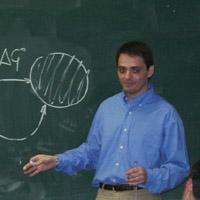
Carbon-based nanomaterials for ambient monitoring systems
|
|
Speaker
|
Dr. Juan Casanova-Chafer (Chercheur, Chimie des Interactions Plasma-Surface, Université de Mons, Belgique)
|
|
Date
|
5 April 2024
|
|
Time
|
10:30-11:30
|
|
Place
|
工学部5号棟105教室
|
abstract:
Monitoring air pollutants is of paramount importance for safeguarding public health and the environment. In this talk, we will delve into the significance and challenges of creating widespread sensing networks and the utilization of carbon-based nanomaterials as sensing platforms.
While carbon nanomaterials offer remarkable advantages such as high surface area and excellent conductivity, challenges such as limited selectivity and sensitivity persist. To address these limitations, several examples, such as the use of lead halide perovskite nanocrystals for decorating graphene, will be shown.
Additionally, insights into the internationalization and mobility opportunities provided by the European grants for research will be discussed.
○講演会
|
Title
|
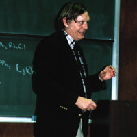
In-situ observation of formation and migration of defects in van der Waals heterostructure
|
|
Speaker
|
Dr. Hanako OKUNO (Chercheur CEA: DRF/INAC/MEM/LEMMA)
|
|
Date
|
28 July 2017
|
|
Time
|
16:10-17:10
|
|
Place
|
工学部5号棟104教室
|
abstract:
Two dimensional (2D) layered structures, such as graphene and transition metal dichalcogenides (TMDs), have attracted much attention for future electronics and optoelectronics due to their unique electronic structures. Recently, tuning the electronic properties of these atomically thin materials has become one of the exciting challenges. The modification of atomic structures by introducing atomic scale ordered defects and/or mechanical strains has been demonstrated as a powerful strategy to control their band structures.
Aberration Corrected Transmission Electron Microscopy (AC-TEM) has become one of the most suitable techniques for structural modification and analysis of 2D materials. The AC-TEM imaging techniques are able to visualize atomic structures of 2D layers and to modify the atomic structure by irradiation. Therefore, we are able to follow atom displacements during the defect formation to study their dynamics.
In this work, we studied the formation and behavior of electron irradiation induced defects in MoSe2/graphene van der Waals (vdW) heterostructures by in situ AC-TEM. A CVD graphene monolayer was used as the substrate to directly grow the MoSe2 monolayer, thus the both layers are stacked with an ideal vdW interface. The vdW heterostructure was irradiated with electron beam, while images were recorded each 0.1 seconds to follow the atom displacements. In first seconds, Se single vacancies were created and accumulate into vacancy line defects. The observed line defects were compared with line defects calculated by density functional theory (DFT). The observed line defects were identified as double vacancy line defect. After the line defects form, they are still mobile in the MoSe2 layer. Local strain was analyzed individually within each monolayer, MoSe2 and graphene, and demonstrated that the creation and migration of line defects in the MoSe2 layer introduce a strong strain in MoSe2 layer, but without significant strain propagation into graphene underneath. The local strain observation indicates the possibility of independent layer engineering by defects and strains in vdW heterostructures.
○講演会
|
Title
|
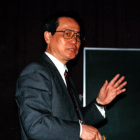
Transmission electron microscopy for atomic scale investigation of two dimensional materials
|
|
Speaker
|
Dr. Hanako OKUNO (Chercheur CEA: DRF/INAC/MEM/LEMMA)
|
|
Date
|
1 August 2016
|
|
Time
|
16:00-17:00
|
|
Place
|
工学部5号棟204教室
|
abstract:
Graphene and other two dimensional materials show great potential for future nano opto-electronics and related applications due to its extraordinary physical properties. The properties of 2D materials are strongly influenced by their atomic structures. Visualizing their structural and chemical configuration at atomic scale is thus essential to understand and further control these atomically thin materials. Recently a low-voltage aberration corrected transmission electron microscopy (LVAC-TEM) has been intensively developed and recognized as the most powerful technique giving an atomic scale imaging of one or few atom thick layer materials. In this talk, LVAC-TEM characterization techniques for the study of 2D materials will be demonstrated.
○講演会
|
Title
|
Solid Oxide Fuel Cells: Point of view on the French policy and presentation of the recent scientific developments at the University of Bourgogne
|
|
Speaker
|
Dr. Lionel Combemale (Université de Bourgogne)
|
|
Date
|
11 November 2015
|
|
Time
|
13:00-14:00
|
|
Place
|
自然科学系総合研究棟2,2Fマルチメディア講義室
|
abstract:
ABSTRACT (pdf)
○講演会
|
Title
|
放射光X線を利用した位置分解XRD法とオペランド分析への応用
|
|
Speaker
|
村山 美乃 博士(京都大学産官学連携本部)
|
|
Date
|
4 August 2014
|
|
Time
|
15:00-15:45
|
|
Place
|
工学部5号棟105教室
|
abstract:
動作環境下の材料中で起きている状態変化をその場測定するため,放射光X線を利用した位置分解XRD法を開発した。本法は,共焦点法と単色化X線のエネルギー走査という放射光X線ならではの技術によって実現したXRDスペクトル測定法である。従来のXRD法(角度走査XRDやエネルギー分散XRD)と比較して,本法は位置敏感性,プロファイル分解能,時間分解能といった点で材料のオペランド分析に対して優れた特長を持っている。
実際に,厚さ100ミクロンのシート状電極中で起きている反応を30ミクロンの空間分解能でその場測定した結果についても紹介する。
|
Title
|
Consortium of CEA-Grenoble/MINATEC/Grenoble INP, for micro and nanotechnologies innovation
|
|
Speaker
|
奥野 華子 博士(原子力・代替エネルギー庁グルノーブル)
|
|
Date
|
4 August 2014
|
|
Time
|
15:45-16:30
|
|
Place
|
工学部5号棟105教室
|
abstract:
2013年から千葉大学工学部と部局間協定を締結したCEA-Grenoble/MINATEC/Grenoble INPというコンソーシアムについて紹介するとともに,ナノキャラクタリゼーションプラットフォームにおけるHAADF-STEM観察成果を紹介する。
○講演会
|
Title
|
Nanofabrication by combining top-down and bottom-up approaches
|
|
Speaker
|
Dr. Laurent VILA (Laboratoire Nanostructures et Magnétisme, INAC/CEA-Grenoble)
|
|
Date
|
24 August 2012
|
|
Time
|
16:00-17:00
|
|
Place
|
工学部5号棟105教室
|
abstract:
In this introductory talk to nanofabrication by lithography techniques we will first review and explain the basic steps of lithography: ie mask fabrication and associated transfer techniques. These basic steps are repeated many times, according to the different materials and levels required in the architecture of the device. Then we will detail different opportunities brought by the combination of top-down and bottom-up approaches for nanofabrication and nano-characterization. First aspect is on the growth and control of the organization of nano-objects, such as patterning of synthesis media or catalyst particles. The second is on the use of top-down techniques for the characterizations of the objects and materials at the nanoscale. The last aspect is on the insertion of nano-objects in the building of nanometre scaled characterization techniques.
Nanofabrication by top-down approach is commonly used by the Information and Communication Technologies to manufacture extremely complex technological products. Some of the amazing achievements are the computer processing units with billion of transistors or the hard disks drives involving different and complex engineering aspects. The basic strategy for the fabrication at the atomic level consists in the fabrication of masks at the surface of the wafer and their transfer in thin films by etching processes.
Research at the laboratory scale is also requiring cutting edge technologies for the nanofabrication and characterization of innovative classes of materials and nanodevices. Top-down approaches are indeed commonly used taking benefit from the tools and processes originally developed for the microelectronic industry. One now well established alternative route to a full top-down approach is the use of smaller building blocks in bottom-up approaches. Some example will be provided during this seminar.
○講演会
|
Title
|
Universitas Gadjah Mada in Approaching a World Class Research University
|
|
Speaker
|
Prof. Sri Juari Santosa (Gadjah Mada University, Department of Chemistry)
|
|
Date
|
4 November 2010
|
|
Time
|
11:00-12:30
|
|
Place
|
工学系総合研究棟2階第1会議室(2F)
|
○講演会
|
Title
|
Control of vertical aligned CNT growth for via interconnects in future integrated circuits
|
|
Speaker
|
奥野 華子 博士(原子力エネルギー庁グルノーブル)
|
|
Date
|
20 August 2010
|
|
Time
|
16:30-17:30
|
|
Place
|
工学部5号棟105教室
|
abstract:
Carbon nanotubes (CNTs) are of much interests for their excellent electrical, optical, thermal and mechanical properties. For instance, quantum computing using individual SWNTs such as for transistor technology has been intensively studied. However, the control of chirality is a serious problem for the use of individual SWCNTs. It is thus still far from realization of devices having the expected performance. Since development of vertical aligned CNT growth technique, the use of large scaled CNT arrays consisting of numerous CNTs have also become an interesting material. Resulting array properties can be controlled by average values of an assemblage of CNTs. This is thus more realistic and opens many possibilities for application.
In this presentation, CNT integration technology towards device applications will be presented, especially focusing on CNT via interconnects. In order to realize high performance CNT based devices, many parameters should be controlled in parallel. Control of direct integration of vertical aligned CNTs in selected devices is essential issue. Grown CNT density is also one of the important parameters to obtain high current density. In this work, a successful CNT growth process for integration in via holes has been developed. The achieved density was higher than 1012 cm-2 in via holes with occupancy more than 50% which is the highest value of currently published ones. The integration process has been tested on various substrate materials which are relevant to real device materials focusing on direct applications. These results positively indicate large possibilities for different type of application. The results have been obtained in the framework of the EU projects Viacarbon (ICT-2007 8.1 216668).
○講演会
|
Title
|
Application of HAADF-STEM analysis for materials science
|
|
Speaker
|
奥野 華子 博士(原子力エネルギー庁グルノーブル)
|
|
Date
|
21 August 2009
|
|
Time
|
17:00-18:00
|
|
Place
|
工学部5号棟105教室
|
abstract:
High-angle annular dark field (HAADF) imaging in a scanning transmission electron microscopy (STEM) has recently demonstrated its potential to provide atomic resolution images altogether with chemical information. The performance of HAADF-STEM has been greatly improved since the practical application of aberration correction technology. The electrical and/or optical properties of devices are often defined by the position of just a few dopant impurities. The observation of individual dopant atoms in the host materials is thus technologically important. As the contrast of HAADF-STEM images is directly related to the atomic number (Z-contrast technique), this technique is becoming a powerful technique to determine the distribution and motion of impurity atoms in materials at atomic resolution. This work specially demonstrates the interest to visualize individual dopant atoms in the real materials using high-resolution HAADF-STEM imaging. In addition, applications of this characterization technique for various materials will be introduced.
○講演会
|
Title
|
深さ分解XAFSで探る表面・界面の構造と磁性
|
|
Speaker
|
雨宮 健太 准教授(高エネルギー加速器研究機構 物質構造科学研究所)
|
|
Date
|
21 July 2009
|
|
Time
|
10:40-12:00
|
|
Place
|
理学部1号館121教室
|
○講演会
|
Title
|
2層カーボンナノチューブの特性評価と,ナノ炭素物質構造制御を目指す高分解能気相移動度測定法の開発
|
|
Speaker
|
菅井 俊樹 准教授(東邦大学理学部)
|
|
Date
|
9 July 2009
|
|
Time
|
17:00-18:00
|
|
Place
|
工学系総合研究棟7階第一会議室(7F)
|
abstract:
ナノ炭素物質はナノ構造に由来する特異な特性を示す。今回紹介する2層ナノチューブは単層ナノチューブの細さと多層ナノチューブの層間相互作用に基づく安定性を兼ね備えたナノ物質である。この2層ナノチューブを生成・精製するわれわれが独自に開発した手法とそれによって得られた高純度・高品質2層ナノチューブの特性評価を示す。
また,これらのナノ炭素物質の構造制御を目指す,高分解能気相移動度測定法とナノ炭素物質に対する適用例,およびその可能性について現在開発中の測定システムと併せて紹介する。
○講演会
|
Title
|
Soluble Polymer Facilitate Homogeneous Catalysis
|
|
Speaker
|
Prof. David E. Bergbreiter (Texas A & M University, USA)
|
|
Date
|
17 March 2009
|
|
Time
|
11:00-12:00
|
|
Place
|
工学系総合研究棟7階第一会議室(7F)
|
references:
1) J. Am. Chem. Soc., 127(41), 14505 (2005)
2) Macromolecules, 40(15), 5337 (2007)
3) J. Phys. Chem. C, 111(25), 8916 (2007)
4) J. Am. Chem. Soc., 129(35), 10666 (2007)
5) Langmuir, 24(8), 4245 (2008)
○講演会
|
Title
|
Highly selective heterogeneous nanocatalyst for the synthesis of pharmaceuticals from clove oil
|
|
Speaker
|
Dr. Silvester Tursiloadi (Senior researcher, Research Center for Chemistry, Indonesian Institute of Sciences, LIPI)
|
|
Date
|
19 November 2008
|
|
Time
|
15:00-16:30
|
|
Place
|
工学系総合研究棟5階第一会議室(5F)
|
abstract:
Nanocatalysts have become increasingly important for the efficient synthesis of active compounds, in particular for the production of fine chemicals and pharmaceuticals. High level of selectivity and efficiency can be achieved using nanocatalysts leading to processes with lower energy level. A unique aspect of nanotechnology is the vastly increased ratio of surface area to volume present in many nanoscale materials, which opens new possibilities in surface-based science, such as catalysis.
This project involves the design of novel nanocatalysts which act as a key in the synthesis of pharmaceuticals. Focus will be on synthesis of eugenol dimmer that can serve as an anti-oxidant and anti-inflammatory drug. The dimmerization of eugenol is an oxidative phenolic reaction that can be carried out with solid acid or metal complex catalyst. These nanocatalysts are characterized as heterogenous catalyst and have advantages in the separation stage of the product which will be very useful for future industrial process. The effect of these catalysts at a nano-structured scale towards the dimmerization reaction and product will be investigated. It has been reported that the dimmer of eugenol, dehydrodieugenol has known to have less cytotoxicity and greater antiinflammatory activity than parent eugenols. Eugenol is a member of the allylbenzene class of chemical compounds. It is a clear to pale yellow oily liquid extracted from certain herbs available in Indonesia especially from clove oil, nutmeg, and cinnamon.
○講演会
|
Title
|
In Situ and Operando Vibrational Spectroscopic Studies of Heterogeneous Catalytic Interfaces
|
|
|
Speaker
|
Prof. Christopher T. Williams (The Department of Chemical Engineering, University of South Carolina)
|
|
Date
|
23 July 2008
|
|
Time
|
11:00-12:00
|
|
Place
|
工学系総合研究棟7階第1会議室
|
○講演会
|
Title
|
魔法数金クラスターの合成と構造・機能
|
|
|
Speaker
|
佃 達哉 教授(北大触セ)
|
|
Date
|
16 November 2007
|
|
Time
|
9:30-10:30
|
|
Place
|
工学部5号棟105教室
|
abstract:
金属クラスターは,その構成原子数(サイズ)に応じて特異的な構造や機能を発現する興味深いナノ化合物である。金属クラスターの合成と評価について,我々の取り組みを中心に紹介する。具体的なトピックスは以下の通り。
1)チオラート保護金クラスターの魔法組成と新しい界面構造の発見
(J. Am. Chem. Soc., 129, 11322 (2007)など)
2)高分子保護金クラスターのサイズ特異的な触媒作用と機能の解明
(J. Am. Chem. Soc., 127, 9374 (2005)など)
○講演会
|
Title
|
Cyclopentadienes and Cyclopentadienyl Complexes with Fluorous Ponytails
|
|
|
Speaker
|
Dr. Jan Čermák (Institute of Chemical Process Fundamentals, AS CR, v.v.i., Czech Republic)
|
|
Date
|
27 July 2007
|
|
Time
|
10:30-12:00
|
|
Place
|
工学系総合研究棟2階第一会議室(2F)
|
abstract:
Various approaches to solving perhaps the most serious problem of organotransition metal catalysis – efficient catalyst recycling – were sought in the past. Nowadays, fluorous biphase catalysis and catalysis in supercritical media belong to modern methods thoroughly investigated recently. Both methods use catalytically active transition metal complexes containg ligands soluble in reaction media with very low polarity. Such ligands typically contain long perfluorinated chains, so called fluorous ponytails. Although many ligand types were already made soluble in fluorous phases (fluorophilized), the most frequent example being phosphines, reports on fluorophilization of cyclopentadienes are scarce. In our labs synthesis and characterization of three independent series of cyclopentadienes and cyclopentadienyl complexes with fluorous ponytails for application in fluorous biphase systems (FBS) and other low-polar media was developed.
○講演会
|
Title
|
無機イオン交換体の新たな展開—イオンふるい作用と剥離反応—
|
|
|
Speaker
|
大井 健太 博士(産総研)
|
|
Date
|
15 September 2006
|
|
Time
|
14:00-15:30
|
|
Place
|
工学部5号棟105教室
|
○講演会
|
Title
|
Mesoporous sulfated titania aerogel prepared by one-step CO2 supercritical extraction
|
|
Speaker
|
Dr. Silvester Tursiloadi (Senior researcher, Research Center for Chemistry, Indonesian Institute of Sciences, LIPI)
|
|
Date
|
27 January 2006
|
|
Time
|
11:00-12:30
|
|
Place
|
工学系総合研究棟5階第一会議室(5F)
|
○講演会
|
Title
|
High Performance Adsorbent based on the Immobilization of Humic Acid on Various Types of Support Material
|
|
Speaker
|
Dr. Sri Juari Santosa (Gadjah Mada University, Department of Chemistry)
|
|
Date
|
19 November 2005
|
|
Time
|
11:00-12:30
|
|
Place
|
工学系総合研究棟5階第一会議室(5F)
|
○講演会
|
Title
|
Non-heme Iron Model Complexes and Intermediates: Oxidation of Olefins
|
|
Speaker
|
金 眞興 教授(韓国,昌原大学工学部)
|
|
Date
|
17 February 2004
|
|
Time
|
11:00-12:00
|
|
Place
|
工学系総合研究棟5階第一会議室(5F)
|
○講演会
|
Title
|
Peat Soil Humic Acid, Its Chemistry and Application
|
|
Speaker
|
Dr. Sri Juari Santosa (Gadjah Mada University, Department of Chemistry)
|
|
Date
|
25 July 2003
|
|
Time
|
13:30-14:30
|
|
Place
|
工学系総合研究棟7階第一会議室(7F)
|
○講演会
|
Title
|
Route from fly ash, natural bentonite and zeolite into hydrocraking catalyst
|
|
Speaker
|
Dr. Yateman Arryanto(Gadjah Mada University, Department of Chemistry)
|
|
Date
|
7 July 2003
|
|
Time
|
14:00-15:30
|
|
Place
|
工学系総合研究棟5階第一会議室(5F)
|
○講演会
|
Title
|
Layered double hydroxides: The interactive host for base and redox catalysis
|
|
Speaker
|
Prof. B. M. Choudary(インド化学技術研究所長代理,触媒部長)
|
|
Date
|
7 March 2001
|
|
Time
|
13:30-
|
|
Place
|
room no. 320, Engineering Bldg. #4
|
○講演会
|
Title
|
酸化チタン光触媒の高効率化と可視光化へのアプローチ
|
|
|
Speaker
|
安保 正一 教授(大阪府立大学)
|
|
Date
|
12 December 2000
|
|
Time
|
16:00-17:00
|
|
Place
|
けやき会館第2会議室
|
○講演会
|
Title
|
Enviromental Catalysis: Some Hints on the Metal-CeO2 Interaction
|
|
|
Speaker
|
Dr. Juan Holgado (Inst. Material Sci. & Tech. Sevilla, Spain)
|
|
Date
|
20 October 2000
|
|
Time
|
15:00-
|
|
Place
|
room no. 103, Engineering Bldg. #2
|
○講演会
|
Title
|
In-Situ Raman Spectroscopy Characterization of Catalysts during the Decomposition of Nitric Oxide
|
|
Speaker
|
Prof. Jack H. Lunsford (Texas A & M University)
|
|
Date
|
18 September 2000
|
|
Time
|
11:00-
|
|
Place
|
room no. 202, Engineering Bldg. #2
|
○講演会
|
Title
|
The Design of Soluble Polymers as Supports for Recoverable, Reusable Homogeneous Catalysts
|
|
|
Speaker
|
Prof. David E. Bergbreiter (Texas A & M University, Department of Chemistry)
|
|
Date
|
13 May 1999
|
|
Time
|
16:00-17:30
|
|
Place
|
Audiovisual Room (3F), Engineering Bldg. #1
|
○特別講義
|
Title
|
環境触媒への期待と課題
|
|
|
Speaker
|
御園生 誠 教授(東京大学大学院工学系研究科)
|
|
Date
|
16 December 1998
|
|
Time
|
16:00-17:00
|
|
Place
|
松韻会館大会議室
|
○特別講義
|
Title
|
均一系錯体触媒による炭素−炭素結合生成反応
|
|
|
Speaker
|
中村 晃 教授(東邦大学,大阪大学理学部名誉教授)
|
|
Date
|
11 December 1998
|
|
Time
|
14:00-15:30
|
|
Place
|
工学部5号棟105講義室
|
|